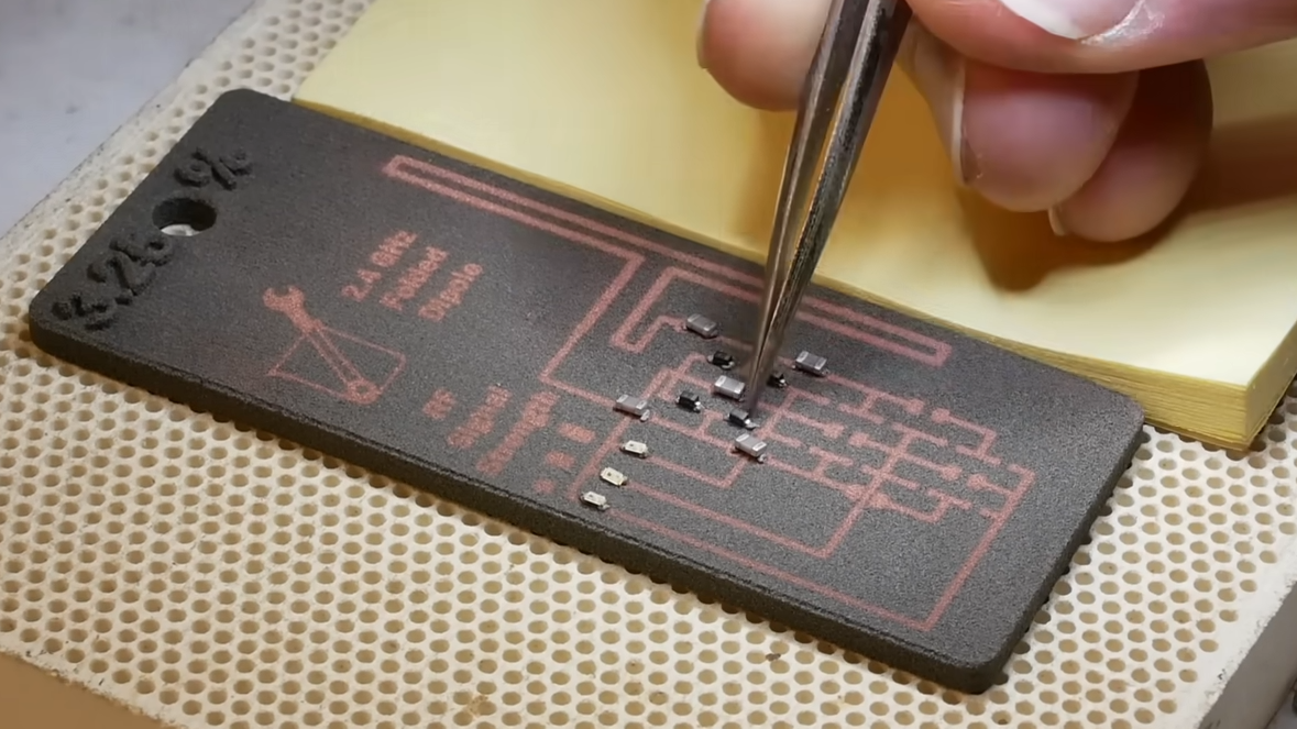
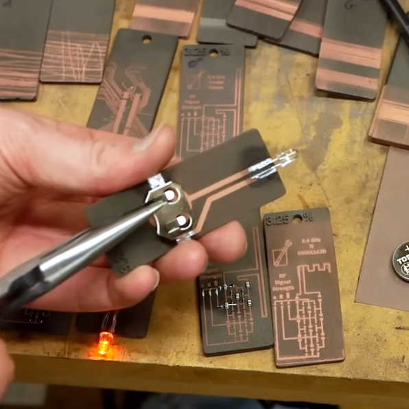
[Ben Krasnow] of the Utilized Science channel just lately launched a video demonstrating his course of for getting copper-plated traces reliably embedded into sintered nylon powder (SLS) 3D printed components, and exhibits off quite a lot of small take a look at boards with traces for useful circuits embedded straight into them.
Right here’s the way it works: The SLS 3D printer makes use of a laser to fuse powdered nylon collectively layer by layer to make a plastic half. However to the nylon powder, [Ben] has added a small quantity of a selected catalyst (copper chromite), in order that prints incorporates this catalyst. Copper chromite is just about inert till it will get hit by a laser, however not the identical type of laser that sinters the nylon powder. Which means after the item is 3D printed, the item is largely nylon with a small quantity of (inert) copper chromite blended in. That units the stage for what comes subsequent.
Activating the copper chromite is all about dumping sufficient power into the particles, and that will get carried out with a pulsed laser. That is how the traces are “drawn” onto the printed object, and these traces shall be copper-clad within the subsequent step.
As soon as the copper chromite catalyst is activated by the second laser, the entire 3D printed object is put right into a chemical tub for electroless copper plating. Once more, solely the locations hit by the pulsed laser find yourself plated. Locations not hit by the second laser stay inert.
There’s an fascinating aspect observe right here. Electroless copper plating is a properly understood course of utilized by each PCB producer on the planet. However the recipes are all proprietary and [Ben] tried with out success to combine up an efficient batch. Ultimately, a chat with OpenAI’s ChatGPT helped crack the case by suggesting a process that labored, saving [Ben] a ton of time. Skip to eight:10 within the video if you wish to know all about that.
The result’s a 3D printed nylon object into which solder-able copper traces are properly and actually embedded. The take a look at items work out nice, however even higher, there’s no purpose the objects and traces even need to be planar. All it could take is a pulsed laser in a position to deal with a curved floor with the intention to create curved traces on a three-d half.
We’ve seen copper-plated 3D printed PCBs earlier than, however that is one thing very totally different and actually elegant. The entire workflow has loads of shifting components, however as soon as managed it’s exceptional repeatable.
[Ben] has truly tried placing copper traces on SLS printed components earlier than, however with solely restricted success. Latest advances in know-how and instruments have actually made the method sing. Watch all of it in motion within the video, embedded under.